A Novel High-Vacuum Die Casting Method for Advanced Gas Sensor Nanofabrication
This technical brief is based on the academic paper "Fabrication of a Pb-Sn Nanowire Array Gas Sensor Using a Novel High Vacuum Die Casting Technique" by Chin-Guo Kuo, Ho Chang, Lih-Ren Hwang, Shu Hor, Jia-Shin Chen, Guo-yan Liu, and Sheng-Cheng Cheng, published in Electronic Materials Letters (2013). It is summarized and analyzed for HPDC professionals by the experts at CASTMAN.
Keywords
- Primary Keyword: High Vacuum Die Casting
- Secondary Keywords: Pb-Sn Nanowire, Gas Sensor, Anodic Aluminum Oxide (AAO), Nanomold, Nanofabrication, Die Casting Technique
Executive Summary
- The Challenge: Traditional methods for fabricating metal nanowires often rely on high-pressure gas injection, a process that poses significant operational dangers.
- The Method: Researchers developed a novel approach using a high-vacuum die casting technique to inject a molten Pb-Sn alloy into a porous Anodic Aluminum Oxide (AAO) nanomold.
- The Key Breakthrough: The study successfully fabricated high-density arrays of Pb-Sn nanowires with a uniform diameter of 80 nm and a length of 50 µm, demonstrating the viability of die casting for nanoscale manufacturing.
- The Bottom Line: This research proves that high-vacuum die casting is a safer and effective alternative for producing one-dimensional nanomaterials, specifically for creating key components for advanced N-type semiconductor gas sensors.
The Challenge: Why This Research Matters for HPDC Professionals
For years, the fabrication of one-dimensional nanomaterials like nanowires has been a complex process. While methods like gas injection have been used to fill AAO templates, they require compressors to supply high-pressure gas. This places the vacuum chamber under high pressure, increasing the operational danger during experiments. To overcome this safety and operational challenge, this study explores a novel approach that leverages the principles of high-vacuum die casting—a technique familiar to many in the manufacturing industry—and applies it to the nanoscale. The goal was to develop a safer, more controlled method for fabricating high-density metal nanowire arrays for advanced applications.
The Approach: Unpacking the Methodology
The researchers employed a multi-step, precision-controlled process:
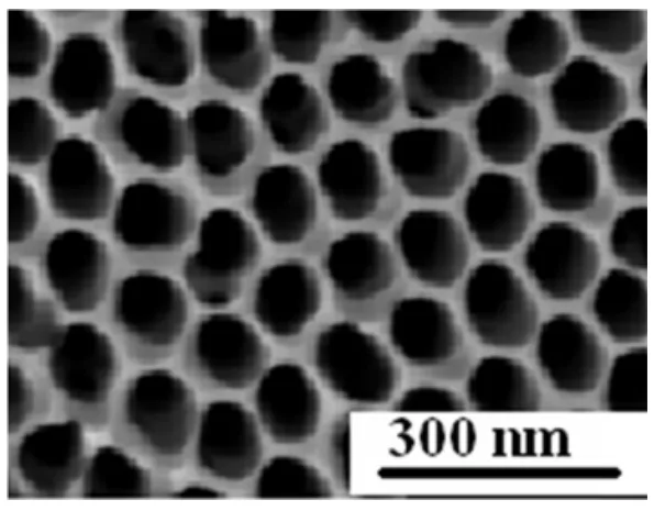
- Nanomold Fabrication: An Anodic Aluminum Oxide (AAO) nanomold was created by etching a high-purity (99.7%) aluminum substrate. This process resulted in a template with highly regular, self-arrayed pores, each measuring 80 nm in diameter (as shown in Figure 2).
- Alloy Preparation: A hypoeutectic Sn-Pb alloy (50% Sn, 50% Pb by weight) was prepared by mixing high-purity metals and smelting them in a high-vacuum environment to prevent oxidation and ensure precise composition.
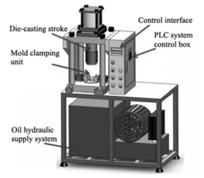
- High-Vacuum Die Casting: The core innovation involved placing the AAO template and the solid Pb-Sn alloy into a custom PLC die casting machine (Figure 1). The system was placed under vacuum (10⁻³ torr), and the alloy was heated until molten. Hydraulic pressure was then applied to inject the molten alloy into the 80 nm nanopores of the AAO template. After solidification, a high-density Pb-Sn nanowire array was formed.
The Breakthrough: Key Findings & Data
The study successfully demonstrated the fabrication of uniform, high-density nanowire arrays using the high-vacuum die casting method.
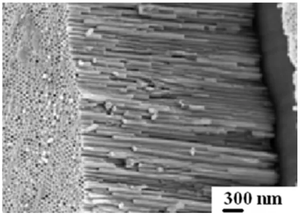
- Uniform Nanostructure: SEM imaging confirmed the creation of a highly ordered AAO template with 80 nm pores (Figure 2). After casting and etching, cross-section SEM images revealed a high-density array of Pb-Sn nanowires that were formed independently and did not contact each other (Figure 3). The final nanowires had a diameter of 80 nm and a length of 50 µm.
- Alloy Composition and Structure: Energy-dispersive X-ray spectroscopy (EDS) confirmed the alloy composition was approximately 49.63% Sn and 50.37% Pb, very close to the target 1:1 ratio. The XRD pattern in Figure 4 showed that the fabricated alloy has a polycrystalline structure.
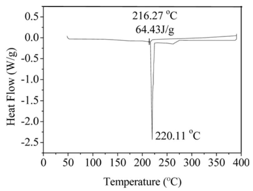
- Thermal Properties: A Differential Scanning Calorimetry (DSC) test determined the melting point of the fabricated Sn 50% - Pb 50% wt. alloy to be 216.27°C (Figure 5), providing critical data for process control.
- Sensor Fabrication: The study concluded by demonstrating how the fabricated nanowire array could be processed into an N-shaped semiconductor gas sensor by depositing copper contacts, as illustrated in the schematic in Figure 6.
Practical Implications for Your HPDC Operations
While this research focuses on the nanoscale, its principles have significant implications for advanced manufacturing and die casting operations.
- For Process Engineers: This study showcases a powerful, safer alternative to high-pressure gas injection for filling intricate, high-aspect-ratio cavities. The use of hydraulic pressure in a vacuum environment offers superior control and eliminates the hazards associated with pressurized gas systems.
- For Quality Control: The precise replication of the 80 nm template features into solid metal nanowires highlights the incredible fidelity achievable with vacuum-assisted die casting. This underscores the potential of the technology for producing net-shape components with extreme precision.
- For Die Design & Advanced Materials: This research pushes the boundary of what is considered "castable." It suggests that die casting principles can be extended to fabricate advanced nanomaterials and components for the electronics and sensor industries, opening up new markets and applications for casting technology.
Paper Details
Fabrication of a Pb-Sn Nanowire Array Gas Sensor Using a Novel High Vacuum Die Casting Technique
1. Overview:
- Title: Fabrication of a Pb-Sn Nanowire Array Gas Sensor Using a Novel High Vacuum Die Casting Technique
- Author: Chin-Guo Kuo, Ho Chang, Lih-Ren Hwang, Shu Hor, Jia-Shin Chen, Guo-yan Liu, and Sheng-Cheng Cheng
- Year of publication: 2013
- Journal/academic society of publication: Electronic Materials Letters
- Keywords: anodic aluminum oxide nanomold, Pb-Sn alloy, array nanowires, vacuum die casting, gas sensor
2. Abstract:
In this study, an anodic aluminum oxide nanomold was obtained by etching on an aluminum substrate at a purity of 99.7% with an oxalic acid electrolyte. After etching, a nanomold was prepared with pores that were measured at 80 nm in diameter. This nanomold was used as a base. Using the vacuum casting method, the Pb-Sn alloy was die-cast into the nanomold and consequently shaped into a Pb-Sn alloy nanowire of 80 nm in diameter and 50 µm in length. After solidification, a Pb-Sn nanowire array was obtained. The array of Pb-Sn nanowires prepared in this study can be applied to a gas sensor. Microstructural analysis of the AAO nanomold and the Pb-Sn nanowire array are performed by SEM and XRD.
3. Introduction:
The introduction highlights the utility of porous templates, specifically Anodic Aluminum Oxide (AAO), for fabricating functional nanostructural materials. AAO offers a self-arrayed, hexagonal structure with uniform pore sizes that can be adjusted from tens to hundreds of nanometers. While methods like gas injection have been used to fill these templates to create nanowires, they require high-pressure gas, which introduces operational danger. This study proposes a novel and safer approach using a high-vacuum die casting technique to fabricate one-dimensional nanomaterials, a method not previously detailed in literature for producing Pb-Sn nanowire arrays.
4. Summary of the study:
Background of the research topic:
The fabrication of nanostructural components often relies on templates with controlled porosity. Anodic Aluminum Oxide (AAO) is an ideal material for this purpose due to its ability to form self-assembled, high-density arrays of uniform pores. This makes it a popular choice for creating nanomaterials.
Status of previous research:
Previous studies have successfully filled AAO templates with materials like bismuth using a gas injection method. However, this method requires a compressor and high-pressure gas, which increases experimental risks. While high-vacuum die casting has been used for bulk parts, its application for fabricating nanowire arrays had not been reported.
Purpose of the study:
The primary purpose was to develop and demonstrate a novel, safer method for fabricating metal nanowires using a high-vacuum die casting technique. The study aimed to produce high-density Pb-Sn alloy nanowire arrays and characterize their structure, with the ultimate goal of applying them as a key component in a gas sensor.
Core study:
The core of the research involved three main parts: 1) Fabricating a porous AAO template with 80 nm pores. 2) Preparing a hypoeutectic Pb-Sn alloy (50% wt. each). 3) Using a custom-developed PLC high-vacuum die casting machine to inject the molten alloy into the AAO template to form a nanowire array. The resulting nanomaterial was then analyzed using SEM, XRD, and DSC to verify its physical and chemical properties.
5. Research Methodology
Research Design:
The research was designed as an experimental fabrication and characterization study. It began with the creation of a nanomold (the AAO template) and the preparation of the casting material (the Pb-Sn alloy). The central part of the experiment was the use of a PLC-controlled high-vacuum die casting machine to force the molten alloy into the nanomold. The final step involved analyzing the resulting nanowire array to confirm its dimensions, composition, and crystalline structure.
Data Collection and Analysis Methods:
- AAO Template Fabrication: A two-stage anode handling process with 0.3 M oxalic acid was used on a 99.7% pure aluminum sheet.
- Alloy Smelting: High-purity (99.9%) Pb and Sn were mixed and smelted at 300°C in a high-vacuum environment (3 × 10⁻⁶ torr) to prevent oxidation.
- Vacuum Die Casting: The AAO template and Pb-Sn alloy were placed in a vacuum die casting mold (10⁻³ torr). The alloy was melted, and normal oil pressure was applied via a PLC die casting machine to inject the metal into the template's nanopores.
- Analysis: Microstructural analysis was performed using Scanning Electron Microscopy (SEM). The alloy's crystalline structure was determined by X-ray Diffraction (XRD). Thermal properties were measured using Differential Scanning Calorimetry (DSC).
Research Topics and Scope:
The research focused on the fabrication and characterization of Pb-Sn nanowire arrays. The scope included the synthesis of the AAO template, the vacuum smelting of the Pb-Sn alloy, the application of a novel high-vacuum die casting technique for nanofabrication, and the microstructural analysis of the final product. The intended application was for an N-shaped semiconductor gas sensor.
6. Key Results:
Key Results:
The study successfully fabricated Pb-Sn alloy nanowire arrays with consistent dimensions. The nanowires were arranged in a high-density array, were formed independently, and did not contact each other. The fabricated nanowires have a diameter of 80 nm and a length of 50 µm. EDS results confirmed the weight percentages of Sn (49.63%) and Pb (50.37%) were close to the intended 1:1 ratio. XRD analysis proved the alloy has a polycrystalline structure. DSC testing showed the alloy's melting point is 216.27°C. The study concluded by proposing a method to create an N-shaped semiconductor gas sensor from the nanowire array.
Figure Name List:
- Fig. 1. Schematic diagram of the PLC die casting machine.
- Fig. 2. SEM image of the AAO template after 3 hours of anode handling for the second time.
- Fig. 3. Cross-section SEM image of the Pb-Sn alloy nanowires in a high-density array structure.
- Fig. 4. XRD pattern of Sn50% - Pb50% wt. alloy.
- Fig. 5. DSC chart of Sn 50% - Pb 50% wt. alloy.
- Fig. 6. Schematic diagram of the prepared Pb-Sn alloy gas sensor.
7. Conclusion:
This study successfully used an aluminum template with a purity of 99.7% to fabricate a porous AAO template. A self-fabricated melted Sn-Pb alloy (Sn 50% - Pb 50% wt.) was injected into the template's nanopores using a vacuum die casting technique to obtain Sn-Pb alloy nanowires in a high-density array structure. The resulting Sn-Pb alloy nanowires had a diameter of 80 nm and a length of 50 µm. The research concludes that this Sn-Pb alloy nanowire array can serve as a key component in a highly sensitive N-shaped semiconductor gas sensor.
8. References:
- O. Jessensky, F. Muller, and U. Gosele, Appl. Phys. Lett. 72, 1173 (1998).
- C. G. Kuo and C. G. Chao, Jpn. J. Appl. Phys. 44, 1155 (2005).
- A. Halimaoui, Y. Campidelli, P. A. Badoz, and D. Bensahel, J. Appl. Phys. 78, 3428 (1995).
- I. Perez, E. Robertson, P. Banerjee, S. B. Lee, and G. W. Rulloff, Small 4, 1223 (2008).
- H. de L. Lira and R. Paterson, J. Memb. Sci. 206, 357 (2002).
- D. Gong and C. A. Grimes, J. Mater. Res. 16, 3331 (2001).
- H. Yamashita and Y. Ichihashi, Appl. Surf. Sci. 121, 305 (1997).
- A. M. Azad and S. A. Akbar, J. Electrochem. Soc. 139, 3690 (1992).
- H. Gan and K. N. Tu, Appl. Phys. 97, 063514 (2005).
- E. S. Kim, K. H. Lee, and Y. H. Moon, J. Mater. Proc. Tech. 105, 42 (2000).
- C. K. Jin and C. G. Kang, J. Power. Sour. 196, 8241 (2011).
- H. A. Patel, N. Rashidi, D. L. Chen, S. D. Bhole, and A. A. Luo, Mater. Sci. Eng. A 546, 72 (2012).
- C. K. Jin and C. G. Kang, Int. J. Hydr. Eng. 37, 1661 (2012).
- S. S. Chee and J. H. Lee, Electron. Mater. Lett. 8, 53 (2012).
- K. H. Kim and I. Amal, Electron. Mater. Lett. 7, 225 (2011).
- Z. Zhibo and Y. Y. Jachie, J. Mater. Res. 13, 1745 (1998).
- Z. Zhang and D. Gekhtman, Chem. Mater. 11, 1659 (1999).
- K. K. Khun, A. Mahajan, and R. K. Bedi, Electron. Mater. Lett. 7, 303 (2011).
Conclusion & Next Steps
This research provides a valuable roadmap for enhancing nanofabrication processes using die casting principles. The findings offer a clear, data-driven path toward manufacturing advanced materials for the electronics industry in a safer, more controlled manner.
CASTMAN is committed to applying cutting-edge industry research to solve our customers’ most challenging technical problems. If the problem discussed in this white paper aligns with your research goals, please contact our engineering team to discuss how we can help you apply these advanced principles to your research.
Expert Q&A:
- Q1: What was the primary problem this research aimed to solve?
- A: The research aimed to solve the operational danger associated with fabricating metal nanowires using the traditional high-pressure gas injection method. It proposed a novel, safer high-vacuum die casting technique as an alternative, as stated in the introduction.
- Q2: What were the final dimensions of the Pb-Sn nanowires fabricated in the study?
- A: The fabricated Pb-Sn alloy nanowires had a diameter of 80 nm and a length of 50 µm. This is mentioned in both the abstract and the conclusion of the paper.
- Q3: How was the final alloy composition verified?
- A: The composition was verified using EDS (Energy-dispersive X-ray spectroscopy). The results, detailed on page 483, showed a weight percentage of 49.63% Sn and 50.37% Pb, confirming the near 1:1 ratio of the hypoeutectic alloy.
- Q4: What is the main advantage of the nanowire array structure fabricated in this study?
- A: The main advantages are that the nanowires are arranged in a high-density array and were formed independently without contacting each other. As stated on page 483, this allows for a greater specific surface area within the same template area, which is beneficial for sensor applications.
- Q5: What is the proposed application for the nanowire array created in this study?
- A: The paper states that the array of Pb-Sn nanowires can be applied as the key component in an N-shaped semiconductor gas sensor with high sensitivity. This is mentioned in the abstract, conclusion, and illustrated in Figure 6.
Copyright
- This material is an analysis of the paper "Fabrication of a Pb-Sn Nanowire Array Gas Sensor Using a Novel High Vacuum Die Casting Technique" by Chin-Guo Kuo et al.
- Source of the paper: DOI: 10.1007/s13391-013-0037-x
- This material is for informational purposes only. Unauthorized commercial use is prohibited.
- Copyright © 2025 CASTMAN. All rights reserved.