This introduction paper is based on the paper "A High Performance Active Antenna for the High Frequency Band" published by "Defence Science and Technology Group".

1. Overview:
- Title: A High Performance Active Antenna for the High Frequency Band
- Author: Wayne Martinsen
- Year of publication: August 2018
- Journal/academic society of publication: Defence Science and Technology Group
- Keywords: Antenna design, High frequency, Distortion, Lightning
2. Abstract:
The paper presents the design of an active antenna operating from low to high frequency (LF to HF), identifying the main sources of inter-modulation distortion and providing recommendations to minimize their generation. It includes a detailed analysis of noise sources within the antenna and their impact on the total output noise, along with discussions on lightning protection. The design is a compact, modular, receive-only antenna suitable for measuring vertical E field strength, general surveillance, and geolocation of HF signals.
3. Introduction:
The paper "A High Performance Active Antenna for the High Frequency Band" addresses the design of broadband vertical monopole antennas used for omni-directional surveillance, HF site noise measurement, and direction-finding arrays. These antennas are typically quiet, with noise primarily from their low DC resistance, but active antennas face challenges from inter-modulation products due to strong RF signals, particularly from AM broadcast stations. The study aims to optimize the antenna’s performance by minimizing distortion and noise while ensuring effective lightning protection.
4. Summary of the study:
Background of the research topic:
Active antennas are critical for HF applications due to their ability to cover a wide frequency range, but they are susceptible to inter-modulation distortion from strong signals and internal noise, limiting sensitivity. The design must balance antenna gain, electronic gain, and noise performance, especially in environments with high RF interference. Lightning protection is also essential to prevent damage from induced voltages in LF to HF ranges.
Status of previous research:
Previous designs often use the U310 JFET for its performance in active antennas, as noted in references like "Low-Noise JFETs-Superior Performance to Bipolars" [Ref. 1]. Literature highlights challenges with inter-modulation products from high-power AM stations and the need for low-noise components, as discussed in "Designing with Field-Effect Transistors" [Ref. 2]. However, there is limited focus on optimizing both noise and distortion while incorporating robust lightning protection.
Purpose of the study:
The study aims to design a high-performance HF active antenna that minimizes inter-modulation distortion, reduces internal noise, and incorporates effective lightning protection. It seeks to provide a compact, modular solution for applications like E field measurement and signal geolocation. The design prioritizes a broadband 50-ohm output impedance to mitigate signal reflections and improve system performance.
Core study:
The research focuses on the design of a receive-only active antenna, detailing the input stage with a U310 JFET, output buffer stage, and lightning protection mechanisms. It analyzes inter-modulation distortion sources, particularly from JFET transconductance variations, and proposes methods to reduce distortion products. Noise sources are quantified, and installation recommendations are provided to optimize performance in various environments.
5. Research Methodology
Research Design:
The study employs a systematic approach to design and test an active antenna, starting with the antenna rod and progressing to the output buffer stage. It uses a common drain JFET configuration to minimize distortion and includes a push-pull output buffer for broadband 50-ohm impedance. The design is tested in a screened room to isolate external EM fields and on an antenna test site for real-world validation.
Data Collection and Analysis Methods:
Data were collected through measurements of frequency response, output intercept points, antenna factor, and noise figure, using setups like those shown in Figure 4.1(a) and (b). A spectrum analyzer with a +30 dB test amplifier was used to measure noise and distortion products, as depicted in Figure 3.9 and Figure 4.3. Calculations, such as those for noise (Equations 3.5, 3.19, 3.20) and antenna factor (Equation 4.2), were implemented in an EXCEL spreadsheet for analysis.
Research Topics and Scope:
The study covers the LF to HF frequency range (10 kHz to 100 MHz), focusing on antenna design, inter-modulation distortion, noise analysis, and lightning protection. It addresses the U310 JFET’s performance, output buffer design, and installation methods to suppress unwanted resonances. The scope includes applications like E field measurement, surveillance, and HF signal geolocation.
6. Key Results:
Key Results:
- The antenna achieves a forward gain of -6.4 dB across the HF band, as shown in Figure 4.2, with a measured antenna factor of 12.8 dB (Figure 4.8).
- Third and second order output intercept points (OPIp3 and OPIp2) were measured at +39.6 dBm and +79.5 dBm, respectively (Figures 4.6, 4.7).
- The calculated excess noise is 6.01 dB at 15.5 MHz (Figure 3.11), closely matching the measured 6.5 dB (Figure 3.10).
- The antenna’s noise figure and spurious free dynamic range (SFDR) were calculated for a 3 kHz bandwidth, showing competitive performance compared to commercial HF receivers (Figure 4.10).
- Lightning protection is achieved using silver mica capacitors and a gas discharge tube, ensuring robustness against induced voltages (Section 2.2.7).
- Installation recommendations, including RF current chokes, suppress unwanted currents below 6.5 MHz (Figures 2.27, 2.28).
Figure Name List:
- Figure 2.3: Variation in transconductance with I_D for the U310 JFET
- Figure 2.4: Test setup and equivalent models for JFET measurements
- Figure 2.5: Variation in voltage gain with two load resistances
- Figure 2.6: Variation in r_ds resistance over g_ds range
- Figure 2.8: Input circuitry of the active antenna
- Figure 2.9: Output Buffer circuitry
- Figure 2.10: Measured return loss at the output terminal
- Figure 2.11: Output buffer circuitry test setup
- Figure 2.12: Frequency response of the output buffer circuit
- Figure 2.13: Measured input impedance of RGS EK890 receiver
- Figure 2.14: Output buffer circuit with 1.8 ohm impedance
- Figure 2.15: Phase and magnitude response with 50 ohm receiver input
- Figure 2.16: Phase and magnitude response with 21 ohm receiver input
- Figure 2.17: Phase and magnitude response with 50 ohm output buffer
- Figure 2.18: Final circuit of the active antenna
- Figure 2.19: Point to point wiring of the active antenna
- Figure 2.20: View showing the recessed BNC connector
- Figure 2.21: Assembled antenna with rod
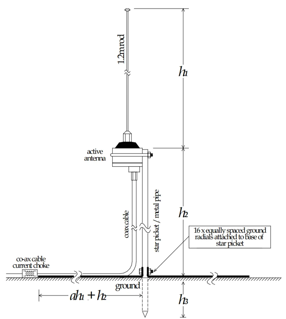
- Figure 2.22: Recommended installation for a given mast height
- Figure 2.23: Recommended lengths of ground radials
- Figure 2.24: Recommended installation for an active antenna
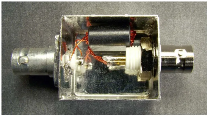
- Figure 2.25: Construction details of current choke
- Figure 2.26: RF current choke housed in a small metal box
- Figure 2.27: Active antenna response with no RF current chokes
- Figure 2.28: Active antenna response with co-axial current chokes
- Figure 2.29: Active antenna response from 10 kHz to 6 MHz
- Figure 2.30: Maximum response at 38 MHz
- Figure 3.1: The three sources of noise in the Active Antenna
- Figure 3.2: Input circuit with 7 uH inductor
- Figure 3.3: Simplified input circuit and Colpitts oscillator
- Figure 3.4: Measured peak in antenna noise floor at 12.26 MHz
- Figure 3.6: Simplified buffer amplifier output circuit
- Figure 3.7: Noise generated by the effective input resistance of the buffer
- Figure 3.8: Noise generated by the FET appearing at the buffer input
- Figure 3.9: Calculated internally generated noise at -88.0 dBm
- Figure 3.10: Measured internally generated noise at -87.5 dBm
- Figure 3.11: Calculated excess noise of 6.01 dB
- Figure 4.1: Two possible methods of connecting to the active antenna
- Figure 4.2: Active antenna output showing forward gain of -6.4 dB
- Figure 4.3: Test set-up for two tone test signal
- Figure 4.4: Two tone test, 8 MHz and 11 MHz
- Figure 4.5: Two tone test set-up for intermodulation products
- Figure 4.6: Third order tone at 5 MHz
- Figure 4.7: Second order tone at 3 MHz
- Figure 4.8: Measured antenna factor
- Figure 4.9: Calculated antenna noise figure
- Figure 4.10: Calculated 3rd and 2nd order SFDR
- Figure 4.11: Calculated strengths of two equal magnitude E fields
7. Conclusion:
The paper successfully presents a high-performance HF active antenna design that minimizes inter-modulation distortion through careful JFET selection and output buffer configuration. It achieves a low noise figure and robust lightning protection, making it suitable for E field measurement, surveillance, and HF signal geolocation. The modular, compact design and installation recommendations ensure practical deployment in various environments.
8. References:
- [1] "Low-Noise JFETs-Superior Performance to Bipolars" (10-Mar-97), Siliconix application note AN108.
- [2] Applications Engineering Staff, Siliconix, Inc. (1990), revised by Ed Oxner, "Designing with Field-Effect Transistors", Mcgraw-Hill, Inc., ISBN: 0-07-053737-1.
- [3] Edwin S. Oxner, (1989), "FET Technology and Application, an introduction", Marcel Dekker, Inc., ISBN: 0-8243-8060-7.
- [4] ARRL (2007-2009), "The ARRL Antenna Book 21" edition", ARRL, ISBN: 0-87299897-6
- [5] Stephen J. Ersi, (1984), "Receiving Systems Design", Artech House Inc, ISBN: 0-89006-135-1)
- [6] Recommendation ITU-R PL372-6, Radio Noise (1994)
- [7] Noll, Edward M., (1975), "FET principles, experiments and projects" ISBN: 0-67221167-X
- [8] Vishay data sheet for U310 FET, Vishay Siliconix Document Number: 70237-550149-Rev. H, 24-Jan-2005
- [9] Martin A. Uman, (2001), "The Lightning Discharge", Dover Publications, Inc., Mineola, New York, ISBN: 0-486-71403-9
- [10] F. R. Connor, (1973), "Noise", Edward Arnold (Publishers) Ltd., 25 Hill Street, London, W1X8RL, ISBN: 0-7131-3066-6
9. Copyright:
- This material is a paper by "Wayne Martinsen". Based on "A High Performance Active Antenna for the High Frequency Band".
- Source of the paper: Not available (No DOI provided in the original document).
- This material is summarized based on the above paper, and unauthorized use for commercial purposes is prohibited.
- Copyright © 2025 CASTMAN. All rights reserved.
Paper Summarize:
The paper "A High Performance Active Antenna for the High Frequency Band" by Wayne Martinsen, published in August 2018 by the Defence Science and Technology Group, details the design of a compact, receive-only active antenna for LF to HF applications. It identifies the U310 JFET’s transconductance variation as the primary source of inter-modulation distortion and implements a common drain configuration with a push-pull output buffer to achieve a broadband 50-ohm impedance, reducing distortion and reflections. The antenna’s noise figure, calculated at 6.01 dB (Figure 3.11), and robust lightning protection make it suitable for E field measurement, surveillance, and signal geolocation.
Key questions and answers about the research:
Q1. What is the primary source of inter-modulation distortion in the active antenna?
A1. The main source of inter-modulation distortion is the variation in the U310 JFET’s transconductance (g_ds) with drain current, as detailed in Section 2.2.5 and Figure 2.3 of "A High Performance Active Antenna for the High Frequency Band."
Q2. How does the antenna achieve a broadband 50-ohm output impedance?
A2. A push-pull output buffer configuration with matched transistors and a 50-ohm termination resistor ensures a broadband 50-ohm output impedance, as described in Section 2.3 and shown in Figure 2.9.
Q3. What measures are taken to protect the antenna from lightning?
A3. Lightning protection is achieved using two 220 pF silver mica capacitors, a gas discharge tube, and a 4 M7 resistor to bleed static charge, as outlined in Section 2.2.7 and Figure 2.8.
Q4. What is the antenna’s measured antenna factor, and how was it validated?
A4. The measured antenna factor is 12.8 dB, calculated using Equation 4.2 and validated through field experiments with a Rohde & Schwarz HE010 system, as shown in Figure 4.8 (Section 4.3).
Q5. How does the antenna’s noise figure compare to commercial HF receivers?
A5. The antenna’s calculated excess noise of 6.01 dB at 15.5 MHz is comparable to some commercial HF receivers for amateur use, though military-grade receivers may require additional amplification (Section 3.4, Figure 3.11).
Q6. What installation methods are recommended to optimize antenna performance?
A6. Recommended installations include ground-level mounting with a metallic mat, elevated mounting with a metal pole, or with ground radials, using RF current chokes to suppress unwanted currents below 6.5 MHz, as detailed in Section 2.6 and Figures 2.22–2.28.