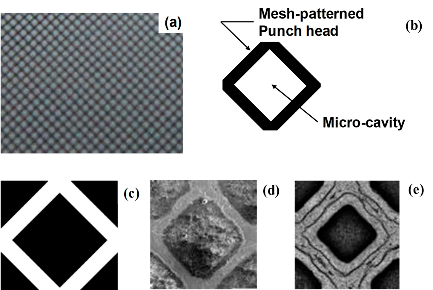
Figure 5. A plasma printing procedure with aid of the low temperature plasma nitriding. (a) CAD
design on the mesh-patterned punch head, (b) a unit cell of mesh-pattern, (c) a unit cell on the
screen-film for screen printing, (d) a nitrided unit cell of microtextures on the die surface at 673 K for
14.4 ks, and (e) a unit cell of mesh-patterned die after sand-blasting