重度の塑性変形(SPD)技術が金属部品の耐食性と硬度をいかに向上させるか:最新研究の解説
本技術概要は、Konrad Skowron氏による学術論文「Properties of the nanocrystalline layers obtained by methods of severe plastic deformation in metals and alloys for biomedical applications」(2021年)に基づいています。HPDC専門家のために、CASTMANのエキスパートが要約・分析しました。
![Figure 2.3 Schematic of a low and high angle grain boundary and the angle of misorientation [8].](https://castman.co.kr/wp-content/uploads/image-2527.webp)
キーワード
- 主要キーワード: 重度の塑性変形(SPD)による表面改質
- 副次キーワード: ナノ結晶層, 表面機械的アトリション処理(SMAT), レーザーショックピーニング(LSP), 耐食性向上, マイクロ硬度, 生体医療用金属, 陽電子消滅分光法(PAS)
エグゼクティブサマリー
- 課題: 金属部品の故障は、多くの場合、疲労、摩耗、腐食といった表面から始まる現象が原因です。特に高性能が求められる用途では、表面特性の向上が不可欠です。
- 手法: 本研究では、重度の塑性変形(SPD)技術である表面機械的アトリション処理(SMAT)とレーザーショックピーニング(LSP)を用いて、マグネシウム、チタン、316Lステンレス鋼の表面にナノ結晶層を形成しました。その特性評価には、陽電子消滅分光法(PAS)などの先進的な分析手法が用いられました。
- 重要なブレークスルー: SPD処理によって導入された結晶格子欠陥(転位や空孔クラスターなど)の濃度と、材料の耐食性向上との間に明確な相関関係があることが実証されました。
- 結論: SMATやLSPのようなSPD技術は、母材の化学組成を変えることなく、表面の微細構造を制御し、硬度や耐食性といった機械的・化学的特性を大幅に向上させるための強力なツールです。
課題:なぜこの研究がHPDC専門家にとって重要なのか
高性能な金属部品の寿命と信頼性は、その表面特性に大きく左右されます。特に、疲労破壊、摩耗、腐食といった劣化プロセスは、部品の表面から発生することがほとんどです(Introduction, p. 17)。従来、物理蒸着(PVD)や化学蒸着(CVD)のような表面コーティング技術が用いられてきましたが、基材との密着性に課題が残る場合があります。
これに対し、重度の塑性変形(SPD)を基盤とする表面改質技術は、部品自体に大きな塑性ひずみを加えて表層を自己的にナノ結晶化させるため、基材と一体化した強固な改質層を形成できるという利点があります(Introduction, p. 17)。この技術がもたらす微細構造の変化と、それが硬度や耐食性といった最終的な部品性能にどう影響するのかを理解することは、次世代の高性能部品開発において極めて重要です。
アプローチ:研究手法の解明
本研究では、生体医療用途で注目されるマグネシウム、チタン、316Lステンレス鋼を対象に、2つの代表的なSPD表面処理法を適用しました。
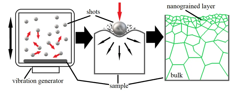
- 表面機械的アトリション処理(SMAT): 振動発生装置によって多数の硬質ボールを高速で試料表面に繰り返し衝突させ、表層に大きな塑性ひずみを導入し、ナノメートルスケールの結晶粒微細化を誘起する技術です(
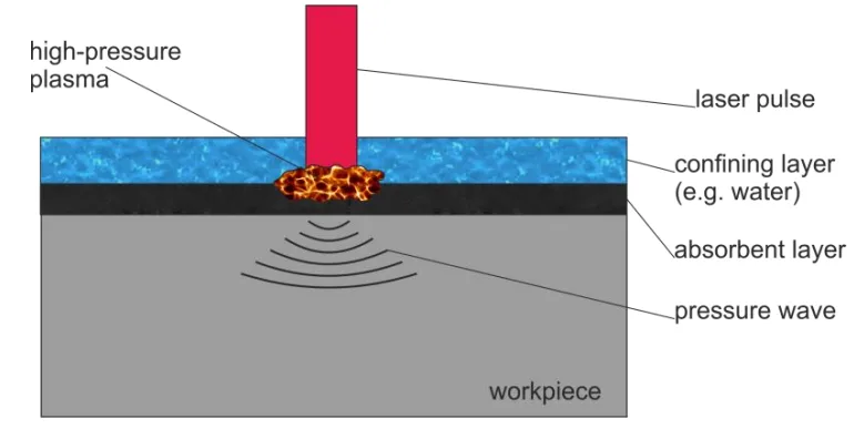
Chapter 3.3.1, p. 45)。 - レーザーショックピーニング(LSP): 高出力のパルスレーザーを試料表面に照射し、その際に発生するプラズマの急膨張による衝撃波を利用して、表層に圧縮残留応力と高密度の欠陥を導入する技術です(
Chapter 3.3.2, p. 46)。
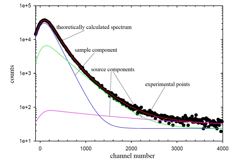
これらの処理によって形成されたナノ結晶層の内部構造、特に結晶格子欠陥の種類と分布を評価するため、本研究では陽電子消滅分光法(PAS)というユニークな分析手法が中心的に用いられました(Abstract, p. 7)。PASは、材料中の空孔(原子空孔)や転位といった微小な欠陥を非破壊で高感度に検出できるため、塑性変形によって導入された欠陥構造を詳細に解明するのに適しています。このほか、マイクロ硬度試験、X線回折(XRD)、電子後方散乱回折(EBSD)、電気化学的腐食試験などが組み合わせて用いられました。
ブレークスルー:主要な研究結果とデータ
本研究により、SPD処理が各種金属の表面特性に与える影響について、以下の重要な知見が得られました。
- 発見1:マグネシウムの特性向上: SMAT処理により、マグネシウムの表面に約800-900μmの深さに及ぶ硬化層が形成されました。この層は、微細な結晶粒と高密度の双晶から構成されており、参照材と比較してマイクロ硬度が最大1.8倍に向上しました(
Chapter 7.3.3, p. 104)。さらに、この微細構造はより安定した水酸化物不動態皮膜の形成を促進し、結果として耐食性が向上することが電気化学的測定によって示されました(Chapter 7.3.6, p. 116)。 - 発見2:チタンにおける耐食性と欠陥構造の相関: チタンにおいても、SMAT処理は耐食性を大幅に向上させました。特に処理時間が長い(120秒)サンプルでは、より顕著な改善が見られました(
Table 9.3, p. 147)。PASによる詳細な欠陥分析から、表層には転位と3~4個の原子空孔からなるクラスターが高密度で存在することが明らかになりました。この高密度の欠陥構造が、強固な不動態皮膜の核生成サイトとして機能し、優れた耐食性をもたらすことが示唆されました(Chapter 9.4 Summary, p. 148-149)。 - 発見3:316Lステンレス鋼の構造変化: LSP処理により、316Lステンレス鋼の結晶粒径は参照材の2735nmから24nmへと劇的に微細化されました。また、高密度の転位や空孔クラスターの導入に加え、変形誘起マルテンサイト相の生成も確認されました(
Chapter 8.3, p. 124-125)。PASによる分析から、LSPによって誘起された欠陥層の深さは約80μmであることが特定されました。
実践的な示唆:あなたのHPDCオペレーションへの応用
本研究は生体医療用金属を対象としていますが、その知見は、自動車、航空宇宙、エレクトロニクス分野など、高い表面耐久性が求められるダイカスト部品にも応用可能です。
- プロセスエンジニアへ: SMATのような表面処理技術は、ダイカスト成形後の二次加工として、部品の硬度と耐食性を飛躍的に向上させる可能性があります。特に、摩耗や腐食が懸念される重要部品に対して有効なソリューションとなり得ます。
- 品質管理へ: 本研究で用いられたPASは、材料の微細な欠陥構造が最終的な性能に直結することを示しています。これは、単純な表面粗さや外観検査だけでなく、マイクロレベルの構造を理解し管理することの重要性を浮き彫りにします。
- 金型・部品設計へ: 表面から破壊が始まる部品において、SPD技術は母材の特性を維持しつつ、表層のみを選択的に強化する設計を可能にします。これにより、部品全体のコストを抑えながら、必要な部分の耐久性を確保するという、より高度な部品設計が実現できます。
論文詳細
Properties of the nanocrystalline layers obtained by methods of severe plastic deformation in metals and alloys for biomedical applications
1. 概要:
- 論文名: Properties of the nanocrystalline layers obtained by methods of severe plastic deformation in metals and alloys for biomedical applications
- 著者: Konrad Skowron
- 出版年: 2021
- 発行機関: The Henryk Niewodniczański Institute of Nuclear Physics Polish Academy of Sciences and Jerzy Haber Institute of Catalysis and Surface Chemistry Polish Academy of Sciences (PhD Thesis)
- キーワード: nanocrystalline materials, severe plastic deformation, SMAT, LSP, positron annihilation spectroscopy, corrosion resistance, biometals
2. 要旨:
本論文の主な目的は、重度の塑性変形(SPD)によって導入された結晶格子欠陥が、生体医療用金属、特にその耐食性にどのように関連しているかを研究することである。研究対象は、表面機械的アトリション処理(SMAT)およびレーザーショックピーニング(LSP)によって、マグネシウム、チタン、316Lステンレス鋼に生成されたナノ結晶トップレイヤーを持つ傾斜微細構造である。主要な研究手法である陽電子消滅分光法(PAS)を、マイクロ硬度試験、電子後方散乱回折(EBSD)、X線回折(XRD)、表面粗さ試験、耐食性試験と組み合わせ、SMATおよびLSPが材料特性に与える影響を評価した。PASにより、変形した表層の欠陥深さ分布が得られ、観察された微細構造、マイクロ硬度プロファイル、残留応力と比較された。SMATがマグネシウムとチタンの耐食性を向上させ、研究対象材料の欠陥濃度と耐食性の間に相関があることが示された。
3. 序論の要約:
高齢化社会に直面し、人工関節などに使用できる安全で耐久性のある材料への関心が高まっている。インプラントの故障は通常、疲労、摩耗、腐食の結果として表面から始まる。この破壊プロセスは、インプラント表面にナノ結晶構造を形成する様々な表面改質法を適用することで遅らせることができる。近年、重度の塑性変形(SPD)に基づく手法が人気を集めている。これらの手法は、基材との密着性が高い超微細粒層を形成する。本研究では、特にSMATとLSPに焦点を当て、これらの手法が材料の構造と特性に与える影響を、陽電子消滅分光法(PAS)を主軸として多角的に調査する。
4. 研究の要約:
研究トピックの背景:
金属部品の性能は、その微細構造、特に表面の構造に大きく依存する。SPDは、材料に大きな塑性ひずみを加え、結晶粒をナノメートルレベルまで微細化する技術群である。これにより、強度や硬度などの機械的特性が向上することが知られている。
従来の研究の状況:
SMATやLSPのような表面ナノ結晶化(SN)技術は、Luらによって概念化されて以来、多くの研究が行われてきた(Ref. [25] in Chapter 3)。これらの技術が硬度や疲労寿命を改善することは広く知られているが、耐食性への影響や、その根底にある欠陥構造との直接的な関係については、まだ完全に解明されていない。
研究の目的:
本研究の主目的は、SPDによって導入された結晶格子欠陥の存在が、生体材料の特性、特に耐食性とどのように相関しているかを明らかにすることである(Abstract, p. 7)。
中核研究:
マグネシウム、チタン、316Lステンレス鋼に対し、SMATまたはLSP処理を施し、形成された傾斜ナノ結晶層の特性を評価した。
- マグネシウム (Chapter 7): SMAT処理(60秒、120秒)を施し、表面形態、微細構造、マイクロ硬度、欠陥構造(PAS)、耐食性を評価した。
- 316Lステンレス鋼 (Chapter 8): LSP処理を施し、結晶子サイズ、欠陥構造(PAS、VEP)を評価した。
- チタン (Chapter 9): SMAT処理(60秒、120秒)を施し、マグネシウムと同様の項目について評価した。
- 熱安定性 (Chapter 10): SMAT処理および静水圧押出(HE)で作製したチタンと316L鋼のナノ結晶材料の熱安定性を、等時焼なましとPAS測定により評価した。
5. 研究方法論
研究デザイン:
参照材(未処理・焼なまし材)とSPD処理材(SMAT、LSP)の特性を比較する実験的アプローチ。処理パラメータ(時間、振幅など)を変え、その影響を評価した。
データ収集・分析方法:
- 表面・微細構造: 光学顕微鏡、SEM、EBSD、XRD、光学プロファイロメーター
- 機械的特性: クヌープマイクロ硬度計
- 欠陥構造: 陽電子消滅寿命分光法(PALS)、ドップラーブロードニング分光法(DB)、可変エネルギー陽電子ビーム(VEP)
- 耐食性: 開回路電位(OCP)測定、電気化学インピーダンス分光法(EIS)
研究対象と範囲:
- 材料: 市販純マグネシウム、チタン(グレード2)、AISI 316Lステンレス鋼
- 処理: SMAT、LSP、静水圧押出(HE)、一軸圧縮
- 評価項目: 表面粗さ、微細構造、結晶子サイズ、格子ひずみ、残留応力、マイクロ硬度、欠陥の種類と分布、耐食性、熱安定性
6. 主要な結果:
主要な結果:
- SMAT処理はマグネシウムとチタンの耐食性を向上させた。この効果は、処理によって導入された高密度の結晶欠陥が、より緻密で保護的な不動態皮膜の形成を促進するためであると結論付けられた。
- PAS測定により、SMATおよびLSP処理された材料の表層には、転位と数個の原子空孔からなるクラスターが高密度で存在することが明らかになった。
- SMAT処理によって形成される硬化層および欠陥層の深さは、マグネシウムで約800-900μm、チタンで約250-400μmであり、材料によって大きく異なることが示された。
- チタンのナノ結晶材料の焼なまし過程では、2つの異なる段階(低温側での空孔クラスターの消滅、高温側での転位の回復)が観測された。
図の名称リスト:
- Figure 1.1: [Not provided in source]
- Figure 2.1: Point defects in a crystal lattice: a) an intrinsic defect – a vacancy, b) an extrinsic defect – an interstitial atom.
- Figure 2.2: Schematic diagram of an: a) an edge dislocation in 2D in a simple cubic structure, the dotted plane is a slip plane, b) a screw dislocation in 3D in a cubic structure.
- Figure 2.3: Schematic of a low and high angle grain boundary and the angle of misorientation.
- Figure 3.1: Surface nanocrystallization methods.
- Figure 3.2: A conceptualization of the SMAT method.
- Figure 3.3: A schematic diagram of the mechanism of the LSP procedure.
- Figure 4.1: 22Na isotope decay scheme.
- Figure 4.2: Positron-electron pair annihilation in a) the center of mass reference frame, b) in the laboratory frame of reference.
- Figure 4.3: Schematic representation of the positron interaction potential with positively charged ions, and defects of the crystal lattice.
- Figure 4.4: Scheme of positron lifetime measurement.
- Figure 4.5: Scheme of a positron lifetime spectrometer.
- Figure 4.6: Positron lifetime spectrum in a logarithmic scale in a function of time, the channel number corresponds to the time.
- Figure 4.7: Schematic illustration of the detector setup used for DB spectroscopy.
- Figure 4.8: DB of the annihilation line. The marked areas denote the intervals used to calculate the S- and W-parameter.
- Figure 4.9: The scheme of positron injector at the VEP facility.
- Figure 6.1: Optical microscope image of the reference sample (a) and the one sandblasted under 5 bar for 1 minute (b).
- Figure 6.2: Values of the S-parameter as the function of the depth from the Cu surfaces exposed to sandblasting.
- Figure 6.3: The dependence of the S-parameter in the function of the depth from the surface for the specimens subjected to cutting and 72% compression.
- Figure 7.1: Mg specimen after the SMAT.
- Figure 7.2: Surfaces of the magnesium specimen subjected to SMAT.
- Figure 7.3: Orientation of the scattering vector K is defined by the φ and ψ angles.
- Figure 7.4: Penetration depth of X-ray radiation in the function of sin²ψ for the single-angle measurement.
- Figure 7.5: Knoop hardness indenter imprint.
- Figure 7.6: Photography of the glass-and-PTFE cell with a platinum foil as the CE and the SCE as the RE.
- Figure 7.7: Optical profiler images of Mg samples surface SMATed for (a) 60 s and (b) 120 s.
- Figure 7.8: The SEM-EDS spectrum for the a) reference sample, b) region of interest.
- Figure 7.9: The EDS spectrum for the a) sample SMATed for 120s, b) region of interest.
- Figure 7.10: Image quality microstructure reconstructed from EBSD of the cross-sectioned specimen of Mg SMATed for 60 s.
- Figure 7.11: a) Optical microscopy image of a typical microstructure on the cross-section of the sample SMATed for 120 s; (b) the Image Quality Microstructure reconstructed from EBSD measurements...
- Figure 7.12: Dependencies of lattice spacing in the function of sin²ψ for a) sample SMATed for 60 s and b) SMATed for 120 s.
- Figure 7.13: The relative microhardness of magnesium samples SMATed for 120 s and 60 s versus depth.
- Figure 7.14: The mean positron lifetime profiles.
- Figure 7.15: Mean positron lifetime values as a function of thickness reduction for the Mg specimen deformed using the uniaxial-hydraulic press.
- Figure 7.16: The S-parameter as a function of incident positron energy (mean implantation depth).
- Figure 7.17: Wr-parameter as a function of S-parameter.
- Figure 7.18: EEC applied in the interpretation of the data from electrochemical impedance spectroscopy measurements.
- Figure 7.19: An example of the fit of the EEC showed in Fig. 7.18 to the impedance data.
- Figure 7.20: Linear sweep voltammetry on the Mg sample not subjected to any treatment (reference sample), the samples SMATed for 60 s and 120 s...
- Figure 8.1: Schematic illustration of LSP procedure; θ = 0.64 mm.
- Figure 8.2: X-ray patterns of 316L samples.
- Figure 8.3: Mean positron lifetime profile.
- Figure 8.4: Positron lifetime components τ₁ and τ₂ and intensity I₂ of the longer component versus depth.
- Figure 8.5: a) The S-parameter as a function of the incident positron energy... b) The W-parameter as a function of the incident positron energy.
- Figure 9.1: Optical profiler images of Ti specimens surface SMATed for (a) 60 s and (b) 120 s, and (c) the reference sample.
- Figure 9.2: EBSD orientation mapping of the cross-section of the Ti SMATed for 120 s.
- Figure 9.3: W-H analysis using PANalytical software.
- Figure 9.4: The microhardness measured on the cross-section of Ti samples SMATed for 120 and 60 s versus the distance from the surface.
- Figure 9.5: Depth profiles of the mean positron lifetime for Ti samples SMATed for 60 s and 120 s.
- Figure 9.6: Evolution of the OCP in time.
- Figure 9.7: Impedance spectra of the as-received SMATed and reference samples.
- Figure 9.8: Impedance spectra for the polished SMATed and reference samples.
- Figure 9.9: Logarithm of modulus of impedance Z versus the logarithm of frequency f in the range of low frequencies for polished SMATed and the reference samples.
- Figure 9.10: Logarithm of modulus of impedance Z versus the logarithm of frequency f in the range of low frequencies for the as-received SMATed and the reference sample.
- Figure 9.11: EEC applied in the interpretation of the data from electrochemical impedance spectroscopy measurements.
- Figure 9.12: Example of the fit to the measured data for the as-received SMAT 120 s sample – Nyquist plot.
- Figure 9.13: Example of the fit to measured data – Bode plots.
- Figure 10.1: Temperature profiles of the S-parameter measured for the HE and the compressed specimens of Ti.
- Figure 10.2: Mean positron lifetime in the function of temperature during isochronal annealing measured for SMATed specimens of Ti.
- Figure 10.3: Temperature dependencies of the positron lifetime components, τ₂(a), τ₁(b), and intensity I₂(c), of the longer component...
- Figure 10.4: Mean positron lifetime in the function of temperature during isochronal annealing measured for SMATed specimens of AISI 316L stainless steel.
7. 結論:
本論文では、SMATおよびLSPによって作製された傾斜微細構造の特性を調査した。
- マグネシウムでは、SMATは転位密度と結晶粒微細化を増加させ、硬度を向上させた。また、陽極酸化に対する感受性を高め、結果としてより優れた耐食性をもたらした。
- チタンにおいても、SMATは耐食性を向上させた。欠陥分布はマグネシウムとは異なり、より浅い領域に集中していたが、高密度の欠陥が耐食性向上に寄与するという共通のメカニズムが示された。
- LSP処理された316L鋼では、2~5個の空孔からなるクラスターが照射面近傍に形成され、高い転位密度が推定された。
- 全体として、PASはSPDによって影響を受ける表層の全範囲を決定するのに有効であり、欠陥濃度と耐食性の間に相関があることを実証した。
8. 参考文献:
- [1] K.V. Rajulapati, C.C. Koch, Nanocrystalline Materials: Mechanical Properties, Reference Module, in: Materials Science and Materials Engineering, Elsevier, 2016.
- [13] K. Lu, J. Lu, Mat. Sci. Eng. A 375 (2004) 38.
- [34] S. Bagheri, M. Guagliano, Surface Engineering, 25 (2009) 3.
- [46] C. Montross. T. Wei, L. Ye, G. Clark, Y. Mai, Int. J. Fatigue 24 (2006) 1021.
- [75] K.D. Ralston, N. Birbilis, C.H.J. Davies, Scr. Mater. 63 (2010) 1201.
結論と次のステップ
本研究は、重度の塑性変形(SPD)が、金属部品の表面特性を根本から改善するためのデータ駆動型アプローチを提供します。特に、微細な欠陥構造の制御が、硬度だけでなく耐食性という化学的特性の向上にも直結することを示した点は、画期的と言えるでしょう。この知見は、より過酷な環境下で長寿命と高信頼性を実現するための明確な道筋を示しています。
CASTMANでは、お客様が直面する最も困難なダイカスト部品の課題を解決するため、常に最新の業界研究を応用しています。本稿で議論された表面改質による性能向上にご関心をお持ちでしたら、ぜひ弊社の技術チームにご相談ください。貴社の部品にこれらの先進的な原理を適用する方法を一緒に検討いたします。
専門家Q&A:あなたの疑問にお答えします
Q1: この研究で、耐食性を向上させるために最も重要だと特定された要因は何ですか?
A1: 本研究では、SMAT処理によって導入された微細な結晶構造と高密度の結晶欠陥が、より緻密で保護的な不動態皮膜(チタンの場合)や水酸化物層(マグネシウムの場合)の形成を促進することが、耐食性向上の最も重要な要因であると結論付けています(Thesis Summary, p. 163-165; Chapter 9.3.5)。
Q2: この研究のアプローチは、従来の表面改質法とどう違うのですか?
A2: 論文のIntroduction(p. 17)によると、PVDやCVDのような従来のコーティング法に対し、本研究で用いられたSPD法は、母材自体を改質するため、形成された層と基材との密着性が本質的に優れている点が大きな違いです。
Q3: この研究結果は、特定の合金にのみ適用可能ですか、それとも広範囲の合金に適用できますか?
A3: 本研究は、Abstract(p. 7)に記載されている通り、市販純度のマグネシウム、チタン(グレード2)、およびAISI 316Lステンレス鋼を対象に実施されました。他の合金への適用性については、さらなる調査が必要となります。
Q4: 研究者たちは、この結論に至るためにどのような特定の測定・シミュレーション技術を使用しましたか?
A4: 研究者たちは、Abstract(p. 7)で述べられているように、結晶格子欠陥を分析するための主要な技術として陽電子消滅分光法(PAS)を用いました。これにより、マイクロメートルオーダーの欠陥分布と性能との直接的な相関を明らかにしました。
Q5: 論文によると、この研究の主な限界や今後の研究課題は何ですか?
A5: 論文のThesis summary(p. 164)では、SMATによってマグネシウムやチタンに誘起される欠陥分布がこれまで決定されていなかったことに言及しており、この分野が新しい探求領域であることを示唆しています。また、チタンの焼なましに関する研究(p. 158)では、空孔クラスターが耐食性に与える影響を確認するにはさらなる研究が必要であると述べています。
Q6: この論文から、ダイカスト工場が得られる直接的で実践的な教訓は何ですか?
A6: 本論文「Properties of the nanocrystalline layers…」から得られる中核的な教訓は、SMATやLSPのような制御された重度の塑性変形を適用することで、部品表面に傾斜したナノ結晶層を形成し、硬度と耐食性の両方を大幅に向上させることが可能であるという点です。これは、研究全体の成果によって強く裏付けられています(Thesis Summary)。
著作権
- 本資料は、Konrad Skowron氏による論文「Properties of the nanocrystalline layers obtained by methods of severe plastic deformation in metals and alloys for biomedical applications」を分析したものです。
- 論文の出典: PhD Thesis, Kraków, 2021.
- 本資料は情報提供のみを目的としています。無断での商業的利用は禁じられています。
- Copyright © 2025 CASTMAN. All rights reserved.